Purification and coatings
High purity graphite
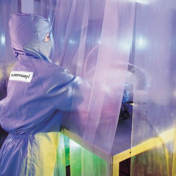
Semiconductor and PV industry controlled with the ETV ICP OES method
Mersen has developed processes designed to significantly improve the physicochemical properties of materials, particularly when required for high-tech applications subjected to high stresses.
Semiconductor and PV industry: high-tech constraints
Purity constraints:
- Our purity processes allow us to achieve extremely low impurity levels, to below 5 ppm.
- The ETV-ICP method is used to detect and monitor impurities to levels below 5 ppb.
Cleanliness constraints:
- Vitreous Carbon Impregnation (VCI) was developed to reduce particle emissions and the vacuum outgassing of materials, particularly for semi-conductor applications.
Resistance to reagents used in plasma processes:
- Mersen products can be coated with a thin layer of pyrolitic carbon thereby reducing the material's permeability to reactive products to a minimum, particularly for semi-conductor applications.
- In order to further enhance the resistance to process reagents, Mersen proposes core impregnation with resin to reduce porosities.
Resistance to hydrogen above 900 °C, MOCVD reagents, and strong acids (HCl, HF)
- Mersen has mastered the deposition of silicon carbide thin films which provides unequalled protection of graphite equipment in particularly harsh environments.
Contact France
Sales & Engineering
F-92231 GENNEVILLIERS France
+33 (0)1 41 85 43 00
Sales & Engineering
Sales & Engineering
PA 15857-1488 St Marys
USA
+1 814 781 1234
Contact France
Sales & Engineering
F-92231 GENNEVILLIERS France
+33 (0)1 41 85 43 00
Sales & Engineering
Sales & Engineering
PA 15857-1488 St Marys
USA
+1 814 781 1234
Product Literature
ETV-ICP OES - detecting limits for high purity carbon and graphite
Download1.82 MB
ETV-ICP OES - detecting limits for high purity carbon and graphiteETV-ICP OES - detecting limits for high purity carbon and graphite
Download1.82 MB
ETV-ICP OES - detecting limits for high purity carbon and graphite